

Applications :
Structure: Mono crystalline
Growing method: CZ/FZ
Type: N/P
Orientation: <111> <100> <110>
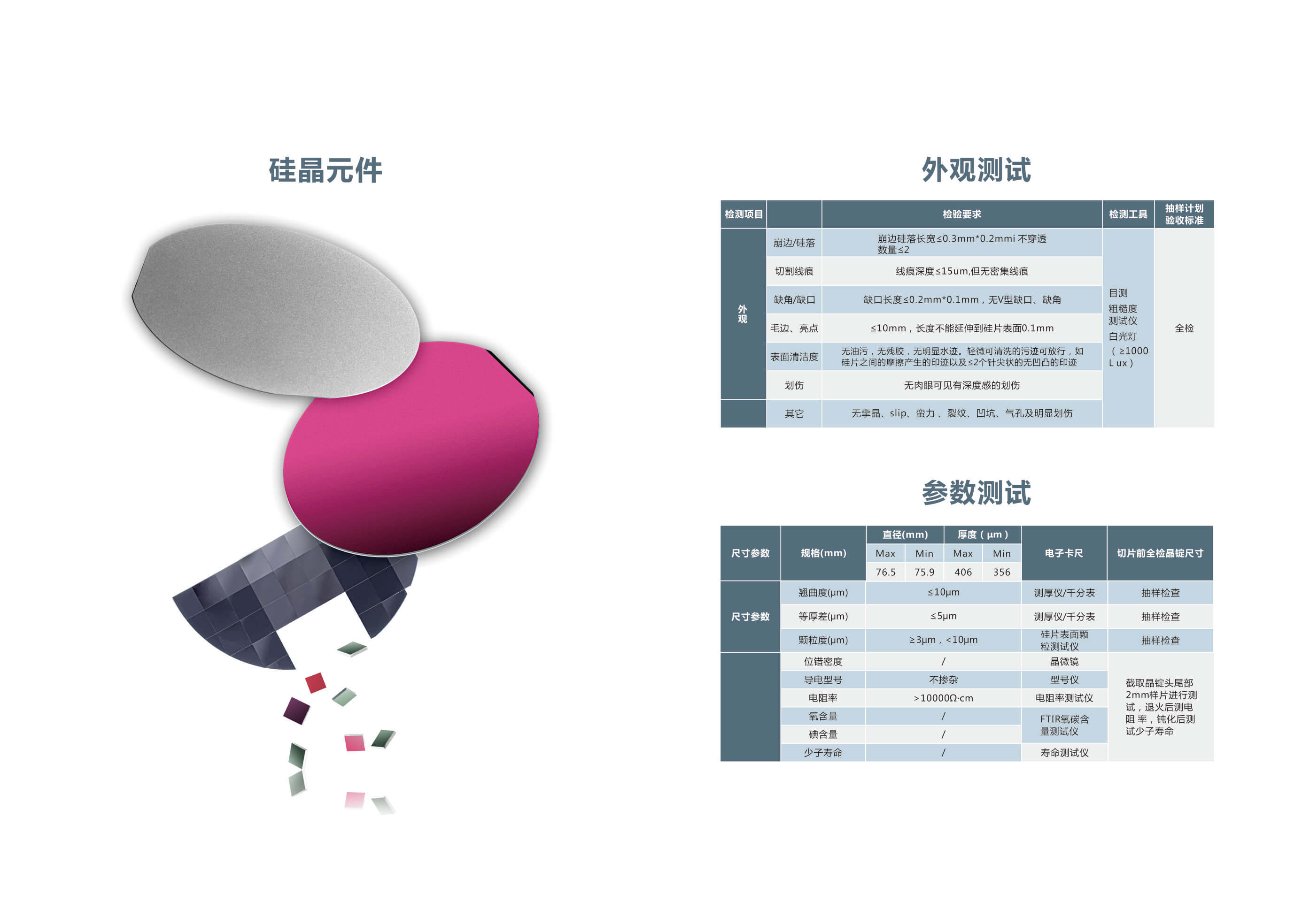
Resistivity: 0.05-10000ohm.cm
Grade: Optical/Mirror/Semiconductor/Tar get
Dislocation density: None
Density: 2.33g/cm3
Melting Point : 1414℃
Transmission range: 1.2-15um
Optical application:band pass filter, thermography, ATR crystal, mirrors,wafer,windows,lenses,ban d pass filter, ATR crystals,etc.
Product Advantage :
公司拥有单线切割机、多线锯床和数控切割机。
公司拥有20多台硅片及其它窗口抛光机。
ICC设有两套超声波清洗,工作人员穿着洁净室工作服,以保护洁净度和颗粒。
Product Parameters :
Intrinsic Crystal Technology, provides standard wafers for the semiconductor industry, optical filters, and IC silicon dioxide.
A. Standard Dimensions: 2 inches, 3 inches, 4 inches, 5 inches, 6 inches, 8 inches, 12 inches (300 mm)
B. Resistivity and use – Whether it is SEMI /IC/FILTER grade
C. Polishing requirements: Surface quality of monocrystal silicon polishes: no channel, no erosion pits, no fog, no regional contamination, no edge breakage, no cracks, no pits, no trenches, no mounds, no knife marks, etc.No area stain, no edge collapse, no crack, no knife mark on the back.
thickness (T), 200-1200 um
total thickness variation (TTV) < 10 um
bending (BOW) < 35 um
WARP degrees (WARP) < 35 um
grinding chengdu: SSP/DSP/lap
resistance range: the smaller the price more expensive,
size range: more is not a standard range prices more expensive
crystal direction: “100”, “111” “110”, if you need reference surface
roughness: standard is less than 0.5 nm
flatness: standard is less than 3 um
D. Oxidation treatment: 50nm ~6000nm (routine: 100nm, 200nm, 300nm, 500nm, 1000nm)
")

S01-V A0")
products and services.


